When it comes to processing ceramics and electronics materials, the right method can amplify electrical properties.
Originally used primarily as insulating materials, technological developments in material science have highlighted the conductive properties of ceramics.
As we discussed in the Introduction to Star Burst, processing or homogenizing particles to nano-level size can improve their efficacy. Processing raw materials for ceramic and electronic applications increases surface area, but many methods can compromise the tubal structure or plate shape of the raw materials. And they take a loooong time to work their magic. A lot of processing options also leave behind grinding media, so purity levels are compromised.

Processing raw materials for ceramic and electronic products.
But Star Burst can process valuable ceramics and electronics materials with minimal contamination.
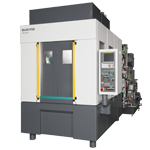
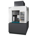
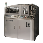
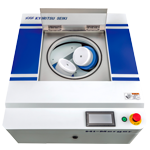
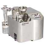
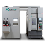
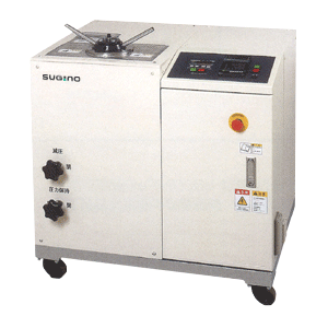
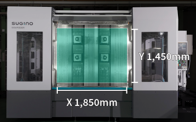
Adjustments to pressure, chamber selections, and the number of passes (along with other finely tuned modifications and factors) can cleanly delaminate or exfoliate without compromising the structural integrity of the material. Quickly. Hours instead of days. And once your R & D has shown you are ready for full-scale production, we have a complete lineup of machines you can count on.
Let’s look at some examples:
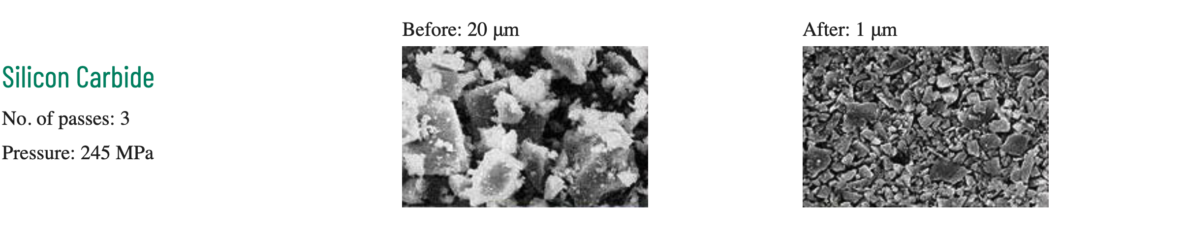
Silicon Carbide
Silicon Carbide has excellent thermal conductivity, low thermal expansion coefficient, and resistance to oxidation at high temperatures, making Silicon Carbide (SiC) nanopowder ideal for ceramics, electronics, semiconductors, and heat-resistant devices. It is also a great abrasive material with high wear resistance.
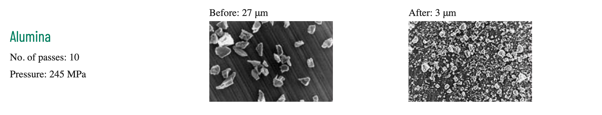
Alumina
Nano-sized alumina, Al₂O₃, can improve the density and smoothness of ceramics, increase thermal fatigue resistance, and is ideal for electrical insulation. Star Burst uses highly pressurized water to process alumina to nano-levels with minimal contamination.
Carbon Nanotubes (CNTs)
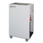
Carbon Nanotubes (CNTs) are extremely cohesive. Dispersal can increase conductivity via increased surface area. Watch how Star Burst Mini disperses CNTs without excess damage to the tube structure.
Graphite
Delamination of graphite improves electrical conductivity, but it needs to be done without disruption to plate shape. Star Burst increases the surface area without damaging the material.
Click to learn more about processing / milling ceramics and electronics materials:
Or watch examples of processing various materials:

And if you can’t find the specific material you are looking for, reach out. Collaboration and testing is available through our US-Based lab facility, and is the foundation of our learning.